The 2nm Race Is Now a Yield Problem, Not a Physics Problem
TSMC and Samsung have both shipped advanced nodes, but the competition has shifted from transistor size to yield and supply chain depth.
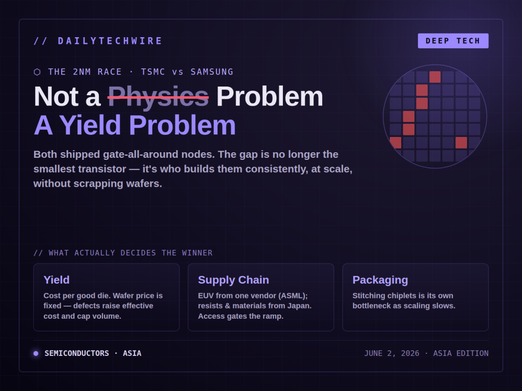
TSMC and Samsung have both moved their most advanced process technologies into production, but the competitive distance between them no longer comes down to who can build the smallest transistor. It comes down to who can build them consistently, at scale, without throwing away too many chips along the way.
That metric, known as yield, has become the central variable in the leading-edge foundry business. A node can be technically impressive and commercially uncompetitive at the same time if too high a share of wafers come off the line defective.
What "new node" actually means now
The industry has moved past the era where shrinking a transistor delivered automatic gains. At the leading edge, both TSMC and Samsung have adopted gate-all-around (GAA) transistor structures, which wrap the channel on all sides to control current leakage that older FinFET designs struggle with at very small dimensions.
The structural change is significant because it resets the manufacturing learning curve. A new transistor architecture means new process steps, new failure modes, and a fresh climb back up the yield curve, even for companies that have spent decades refining the previous approach.
This is where the two companies have historically diverged. Samsung moved to GAA earlier on its 3nm-class process, betting that an early start would build process maturity. TSMC stayed with FinFET longer before transitioning, prioritizing yield stability on high-volume nodes that customers were already buying in quantity.
Why yield decides the winners
For a fabless customer designing a phone or data-center chip, the relevant question is not the marketing name of the node. It is the cost per good die and whether enough working chips can be delivered on the schedule a product launch depends on.
Low yield raises effective cost, because the wafer price is fixed regardless of how many usable chips it produces. It also constrains volume, which matters when a single large customer can absorb much of a foundry's leading-edge capacity. A node with strong yield can win the bulk of premium orders even if a competitor's node looks comparable on paper.
This dynamic explains why the largest mobile and high-performance computing customers have historically concentrated their most advanced designs with whichever foundry demonstrated reliable yield first. Reputation for manufacturing consistency, not specification sheets, drives where the highest-value contracts land.
The supply chain underneath
Leading-edge manufacturing also depends on a narrow set of upstream suppliers. Extreme ultraviolet (EUV) lithography systems, used to pattern the smallest features, come from a single vendor, ASML of the Netherlands. Specialty chemicals, photoresists, and advanced packaging materials draw heavily on suppliers concentrated in Japan and a handful of other locations.
That concentration means a node's competitiveness is not determined inside the fab alone. Access to enough EUV tools, the maturity of advanced packaging lines that stack and connect chiplets, and the stability of materials supply all feed into whether a process can ramp to high volume on schedule.
Advanced packaging has become particularly important as transistor scaling slows. Stitching multiple smaller dies together into one package can deliver system-level performance gains that a single monolithic chip can no longer provide cheaply, and capacity for that packaging step has become its own bottleneck.
The Asia stakes
The leading edge of semiconductor manufacturing remains overwhelmingly concentrated in Asia. TSMC's most advanced production sits in Taiwan, Samsung's in South Korea, with both companies building capacity elsewhere but keeping their newest processes close to home initially. The region holds the largest concentration of advanced fabs, packaging facilities, and the engineering talent that runs them.
That concentration shapes the strategic picture for the rest of the world. Efforts to build advanced fabs in the United States and Europe are under way, but moving a new process to a new site adds its own yield-ramp challenge. The hardest part of the business, getting a leading-edge line to produce reliably, does not transfer easily across geographies.
For developers and chip buyers across Asia-Pacific, the practical effect is that the timing and pricing of next-generation devices remain tied to how quickly these two companies climb their respective yield curves. The node names will keep advancing. Whether the chips arrive on time, and at what cost, is the question that matters.